Sony unveils 12.4 megapixel 10fps APS-C sensor
THE PRESS and trade announcement made below on August 20th 2007 does little to confirm on deny rumours about the forthcoming AA and Flagship DSLRs. Why? You need to study the image, and study the dimension data, and fully understand what they are talking about, before the implications are clear.
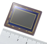
First of all – the chip dimensions given in the table are for the entire CMOS assembly, which is the dark blue area surrounded by a thin gold broken line, shown mounted on a further circuit module. As you can see from the ruler scale, the entire module is approximately 35mm in length – the same as the ‘gate’ of a film camera – and is not a 2:3 ratio in size, so its short dimension would not fit within a 24mm height aperture.
This does not matter much, as DSLRs have no film gate, but it’s clearly a fairly large assembly and may have been mistaken by early leak-posters for full frame because someone has seen the 35mm length on the scale. The active area of the sensor, with its 28.4mm diagonal, is clearly the same as a normal APS-C (Pythagoras confirms this in the backward direction without any problems).
Yet the rumours have been for 14.4 megapixels and APS-C. I have always felt that 12.x megapixels was the target – and I calculated the sensor pixel count by basing it on the R-1 CMOS sensor scaled up to APS-C. That seems to be the basis of the new sensor.
Some rumours have said 10 frames per second, others 5 frames. This technical specification clearly indicates that 10fps is possible, and was probably the source of the figure. I suspect that an Advanced Amateur DSLR might not use the full 10fps capacity, which would call for a very large buffer and might introduce heat-related noise. But we may yet be surprised. Sony could be using this sensor in the new Advanced Amateur model, and they might decide to defeat Canon’s competing 6.5fps by putting in that big buffer.
There is something about the language of this technical release which makes me suspect the AA model has a CMOS sensor one generation earlier than the technology described – too much of this release appears to be about to happen in a medium term future. Production ‘will be carried out’ may be a translation issue, but saying this normally is equvalent to saying ‘production has not yet started’. Since we can be pretty sure the entire production 1st batch of the sensor for the AA model is now completed – it probably happened earlier this year – this wording seems to deny the possibility of the AA model including the IMX201 sensor.
This sensor sounds more than exciting – it sounds like the first of a new generation which will place Sony in the forefront with HD-TV/high resolution digital still/fast sequence shooting DSLRs. This is what market predictions say will eventually replace today’s DSLRs in the hands of newsgatherers. It has the potential to be filming an HD-TV report and capture a still frame separately, during the filming, without interruption, using a second shutter button. It might even be able to capture 10fps still frame bursts, while feeding live HD-TV to a different output.
That would fulfil the dream requirements of news and sports crews. And it wouldn’t half be handy for the rest of us! With Alpha system optics on the front…
– David Kilpatrick
(the release follows)
Tokyo, Japan – Sony Corporation today announced the commercialization of “IMX021”, an APS-C size (diagonal: 28.40mm/Type 1.8) 12.47 effective megapixel ultra-high speed, high image quality CMOS image sensor designed to meet the increasing requirement for rapid image capture and advanced picture quality within digital SLR cameras. Sony will position “IMX021” as a key device capable of generating new added value in the high-growth digital SLR camera market, actively promoting its use within Sony and externally.
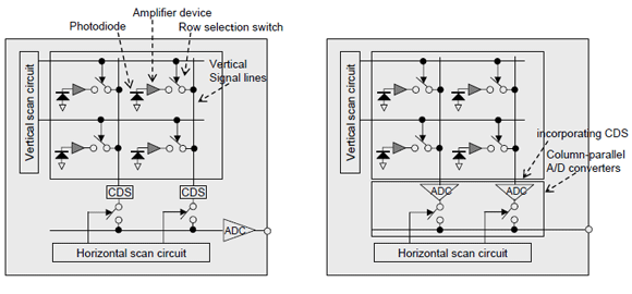
One of the main strengths of CMOS image sensors is their potential for system integration, enabling both analog and digital circuits to be combined on the same chip. “IMX021” maximizes these advantages, while also incorporating Sony’s newly developed “Column-Parallel A/D Conversion Technique”, providing each column within the sensor with its own A/D* converter.
“IMX021” CMOS Image Sensor
This system enables analog signals transferred from the Sensor’s vertical signal lines to be A/D converted directly, over the shortest possible distance. It also minimizes image degradation caused by the noise that arises during analog processing, while at the same time delivering an extremely high signal conversion speed (in all-pixel scan mode) of 10.39 frame/s (12 bit).
Furthermore, since processing is performed in parallel for each column, even if the number of pixels or the frame rate increases, A/D conversion can be performed at significantly lower frequencies than with conventional non-parallel circuit structures. Consequently, high picture quality digital signals can be processed without the noise interference that results from high frequency signals.
The “Column-Parallel A/D Conversion Technique” aligns both digital and CDS* circuits alongside each column. Column-parallel digital CDS circuits reduce not only pixel noise, but also the noise and inter-column processing variations that can affect analog CDS circuits. These circuits also limit A/D converter fluctuations. With this dual noise cancelling technology realizing high-precision noise reduction across both analog and digital circuits, the “IMX021” image sensor allows signals to be transferred, with limited noise, to the image processing circuits of the camera unit itself. This makes it ideally suited for the development of high image quality digital SLR cameras.

Left : Conventional Image CMOS Image Sensor Circuit Structure
Right : Column-Parallel A/D Converter CMOS Image Sensor Circuit Structure
The enhanced quality images generated by “IMX021” are the result of its advanced noise cancelling features based on a unique circuit structure, its pixel array micro-fabrication technologies, and its cleaning and color-filtering capabilities – encapsulating the range of imaging expertise that Sony has accumulated throughout its history of CCD development.
“IMX021” production will be carried out at Sony Semiconductor Kyushu Corporation’s Kumamoto Technology Center.
*A/D : Analog/Digital
*CDS : Correlated Double Sampling
Features
- CDS/PGA Circuit, 12bit-AD Converter on chip
- PGA: Programmable Gain Amplifier
- 12 channel parallel LVDS output
- Readout mode: All-pixel scan mode (12 bit:10.39 frame/s), and Window readout
Device Structure
- Model name: IMX021
- Image size: Diagonal width 28.4mm (Type 1.8)
- Total number of pixels: 4428(H)×2948(V) approx.13.05M pixels
- Number of effective pixels: 4320(H)×2888(V) approx.12.47M pixels
- Number of active pixels: 4312(H)×2880(V) approx.12.41M piixels
- Chip size: 28.0mm(H)×22.3 mm(V)
- Unit cell size: 5.49µm(H)×5.49µm(V)


The press release reads as if use of the sensor is in the future. If it was incorporated in the current (to be announced tomorrow, Thurs) new Nikon or the new Sony (announcement expected soon after), it would have been in production since the beginning of this year, and would have been developed in 2005/6. This release appears to have come from the sensor division, not the DSLR division (the ‘Alpha System Company’ which exists separately within Sony). I think the sensor to be incorporated in the current round of cameras are more likely to be one generation prior to this design. However, we may yet be surprised. Some of the fictitious or speculative leaks of camera specifications – like 10 fps – appear to be based on a leak of this sensor info. If Sony do implement anything faster than 5.5 fps in the advanced amateur model, they will have pulled off a major scoop.
I find two items in the press release to be interesting… First, the use of the word “commercialization”, which, to me, suggests that Sony has in fact been using this sensor in house and is now going to make it available to others. Second is the phrase “actively promoting its use within Sony and externally”, this reinforces the first my thought above and strongly suggests the Sony is using this sensor “somewhere”. Care to guess where?